Datei:Opamptransistorlevelcolored.png
Opamptransistorlevelcolored.png (618 × 488 Pixel, Dateigröße: 10 KB, MIME-Typ: image/png)
![]()
Diese Datei und die Informationen unter dem roten Trennstrich werden aus dem zentralen Medienarchiv Wikimedia Commons eingebunden.
![]()
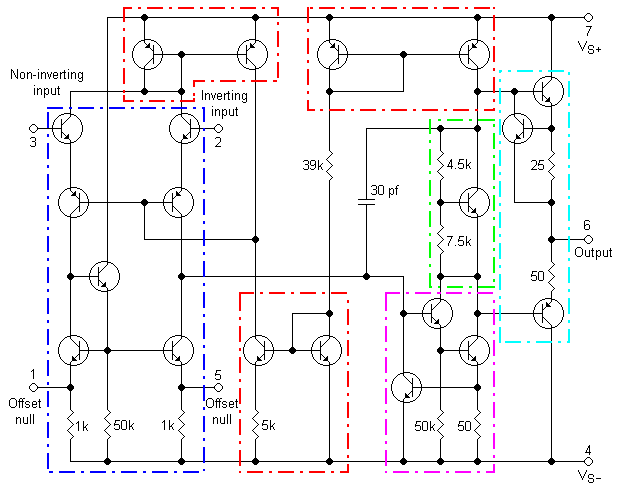
Transistor-level schematic for a 741 op-amp, color coded.
Beschreibung
(See w: Op-amp#Internal_circuitry_of_741_type_op-amp for the most recent description.)
From the diagram, the blue section is a differential amplifier. The base current of the inputs is not really zero, giving the 741 an input impedance of about 2 MΩ.
The sections in red are current mirrors. The input amplifier drives a current mirror load. The top left current mirror allows large common-mode voltages on the inputs without exceeding the active range of any transistor in the circuit. The top right current mirror provides a constant current load for the output circuitry, regardless of the output voltage . The lower current mirror has a very low collector current, because of the 5 kΩ resistor. It is used as a high-impedance connection to the negative power supply, to provide a reference without loading the input circuitry.
The offset null pins are used to remove any offset voltage that would exist at the output of the op-amp when zero signal is applied to the inputs.
The high voltage gain stage is NPN.
The green section is a voltage level shifter. It provides a constant voltage drop between the top and the bottom regardless of supply voltage. If the base current to the transistor is zero, and the voltage between base and emitter (and across the 7.5 kΩ resistor) is 0.625 V (a typical value for a BJT), then the current flowing through the 4.5 kΩ resistor will be the same, and will produce a voltage of 0.375 V. This keeps the voltage across the transistor, and the two resistors at 0.625 + 0.375 = 1 V. This serves as a bias for the two output transistors, to prevent crossover distortion. In some amps this function is achieved with diodes.
The capacitor is used as part of a low pass filter (on the base of an emitter follower) to reduce the frequency response of the amp to prevent oscillations. This technique is called Miller Compensation and functions as an internal capacitive feedback.
The output in cyan is a push-pull emitter follower amplifier. It is driven by a PNP emitter-follower. The output range of the amplifier is about 1 volt less than the supply voltage, since the collector-emitter voltage of the output transistors can never go completely to zero. The resistors in the output mean that the current provided by the output is limited (about 25 mA for the 741), and the output resistance is not zero without feedback. With negative feedback it approaches zero. The output stage has current limiting circuitry.
- Opis wyprowadzeń (cyfry oznaczają numery wyprowadzeń w standardowej obudowie ośmiokońcówkowej, końcówka nr 8 - nieużywana)
- Offset null - balans zera
- Inverting input - wejście odwracające
- Non-inverting input - wejście nieodwracające
- Vs- - minus zasilania
- Offset null - balans zera
- Output - wyjście
- Vs+ - plus zasilania
Op-amp transistor level
-
 Transistor level diagram of an op-amp
 -
 Sectioned transistor level diagram of an op-amp
 -
 Sectioned transistor level diagram of an op-amp with labeled transistors


Created by User:Omegatron using Klunky schematic editor, which the creator considers public domain (possibly with post-editing in the GIMP or Inkscape)
- Dieses Werk darf von dir
- verbreitet werden – vervielfältigt, verbreitet und öffentlich zugänglich gemacht werden
- neu zusammengestellt werden – abgewandelt und bearbeitet werden
- Zu den folgenden Bedingungen:
- Namensnennung – Du musst angemessene Urheber- und Rechteangaben machen, einen Link zur Lizenz beifügen und angeben, ob Änderungen vorgenommen wurden. Diese Angaben dürfen in jeder angemessenen Art und Weise gemacht werden, allerdings nicht so, dass der Eindruck entsteht, der Lizenzgeber unterstütze gerade dich oder deine Nutzung besonders.
- Weitergabe unter gleichen Bedingungen – Wenn du das Material wiedermischst, transformierst oder darauf aufbaust, musst du deine Beiträge unter der gleichen oder einer kompatiblen Lizenz wie das Original verbreiten.

|
Es ist erlaubt, die Datei unter den Bedingungen der GNU-Lizenz für freie Dokumentation, Version 1.2 oder einer späteren Version, veröffentlicht von der Free Software Foundation, zu kopieren, zu verbreiten und/oder zu modifizieren; es gibt keine unveränderlichen Abschnitte, keinen vorderen und keinen hinteren Umschlagtext.
Der vollständige Text der Lizenz ist im Kapitel GNU-Lizenz für freie Dokumentation verfügbar. |
(In short, this means that you can copy and modify the image freely as long as you provide attribution; preferably in the form of a link back to this page.)

|
File:OpAmpTransistorLevel Colored.svg ist eine vektorisierte Version dieses Bildes. Diese sollte an Stelle des Rasterbildes verwendet werden.
File:Opamptransistorlevelcolored.png → File:OpAmpTransistorLevel Colored.svg
Für weitere Informationen siehe Help:SVG. |
 |
Dateiversionen
Klicke auf einen Zeitpunkt, um diese Version zu laden.
| Version vom | Vorschaubild | Maße | Benutzer | Kommentar | |
|---|---|---|---|---|---|
| aktuell | 21:36, 26. Jun. 2005 | | 618 × 488 (10 KB) | Omegatron | An electrical diagram created by User:Omegatron. (Uploaded with Wikimedia Commonplace.) Source: Created by User:Omegatron {{GFDL}}{{cc-by-sa-2.0}} Category:Electrical diagrams\ |
| 21:29, 26. Jun. 2005 |  | 618 × 488 (10 KB) | Omegatron | An electrical diagram created by User:Omegatron. (Uploaded with Wikimedia Commonplace.) Source: Created by User:Omegatron {{GFDL}}{{cc-by-sa-2.0}} Category:Electrical diagrams\ | |
| 01:50, 20. Mai 2005 |  | 618 × 488 (10 KB) | Julo | Operation amplifier 741 {{PD}} from en:wiki |
Dateiverwendung
Keine Seiten verwenden diese Datei.
Globale Dateiverwendung
Die nachfolgenden anderen Wikis verwenden diese Datei:
- Verwendung auf en.wikipedia.org
- Verwendung auf hr.wikipedia.org
- Verwendung auf pl.wikipedia.org
- Verwendung auf sl.wikipedia.org